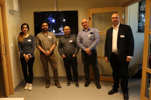
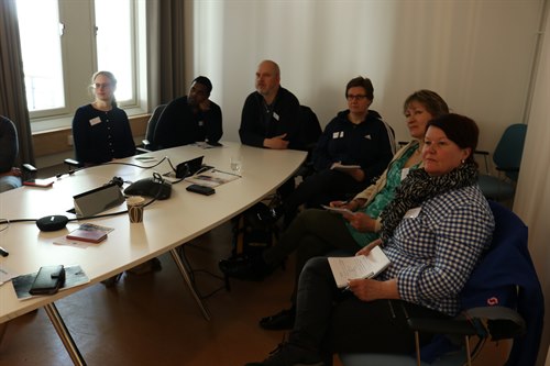
MILAB workshop
On April 26 researchers and companies gathered with suppliers from Horiba, Oxford Instrument and Tescan to develop our knowledge in the new equipments for MILAB.
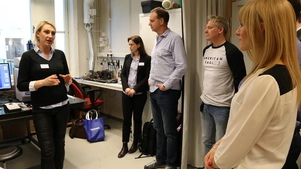
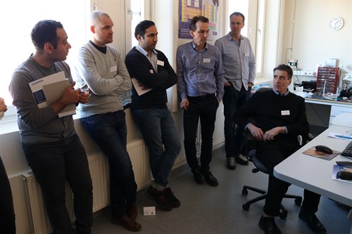
As a continuation of the launch of the Material Innovations Laboratory (MILAB) at Mid Sweden University a dedicated laboratory workshop with focus on scientific equipment were held on April 26, 2018. Each workshop had a dedicated theme and this year's topic was scientific equipment related to optical techniques or research. Suppliers from Horiba, Oxford Instruments and Tescan gave presentations and parallel demonstration sessions during the afternoon. There were also topics on low-voltage techniques in electron microscopy (SEM) together with a SEM-school 'light' hands-on training.
Talk: Horiba Raman Microscopy
The optical inelastic scattering response, raman-scattering, gives characteristic information from bonding and structure of materials, a close relative to this technique is perhaps the more commonly known IR-spectroscopy. Here this raman-technique is combined with an optical microscopy system that brings together these characteristics of the material with a highly resolved lateral position of the sample. That is the method gives answer to what and wear at the same time sort of. The talk will both be both about raman microscopy but also about other related or alternative optical methods.
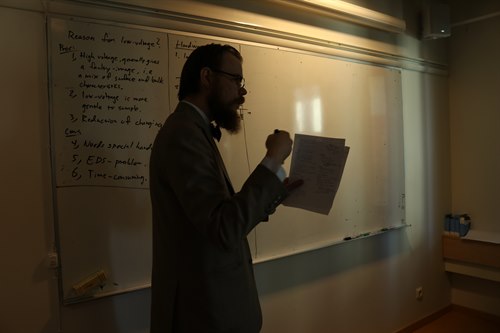
Talk: Oxford Instruments, Low voltage EDS and advantages of WDS detectors over EDS
Energy dispersive Spectroscopy a standard technique for elemental analysis in electron microscopy. Normally this is done at high accelerating voltage of the electron microscope. Research needs of lower accelerating voltage has also brought altered usage of EDS. This talk will be about advantages and drawbacks of low-voltage techniques in EDS-work. Also, WDS, wavelength dispersive spectroscopy, an alternative technique for elemental analysis will be mentioned in the context.
Talk: Tescan, electron microscopy with CL-detectors
Talk: Tescan, general talk on detectorsystems for scanning electron microscopy (SEM) with Cathode Luminescence Cathode Luminescence (SEM-CL) detectors applications. This talk will be both a general talk about special techniques/detectors ad-on’s for SEM such as CL-detectors, but also FIB (focused ion beam) and other advanced techniques will be mentioned. One of the advantages of combining cathode luminescence with electron microscopy is the high lateral resolution in the range of nanometers. Band-gap of semiconductors, plasmon-resonance of nanoparticles, optical active material as fiber optics could be studied with cathode luminescence techniques.
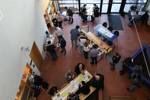
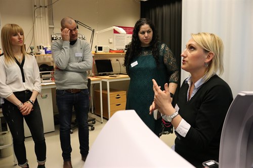
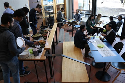
Lunch and poster session FSCN research centre
Lunch will be a buffet-kind-of-thing and there’s room for interaction among the workshop visitors. One goal of the workshop is to bring people together from diverse backgrounds but sharing some common needs. Visitors are therefore suggested to bring posters from there currently ongoing research, company roll-ups or similar for the poster-session.
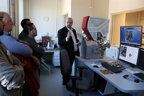
Raman Microscopy
Demonstration of the newly invested raman microscope Xplora plus from Horiba will be made. Both general demonstrations of the capabilities of this type of technique were raman is combined with microscopy as well the special features of this particular machine will be shown.
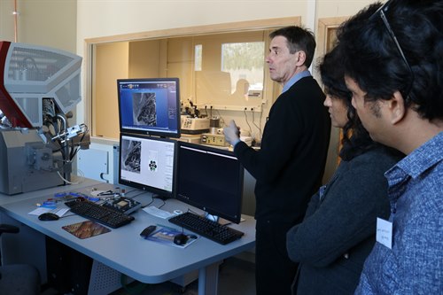
SEM – CL
Cathode Luminescence in scanning electron microscopy will be demonstrated. For the day Tescan brings a demo-detector to show the advantages of this technique combination, its capabilities and limitations. The detector used will be a panchromatic compact CL version.
Low – voltage EDS
EDS is a standard technique for atomic elemental composition studies done together with electron microscopy, traditionally this is conducted at high accelerating voltages settings of the microscope, however there is an ongoing trend of reducing the voltage levels and it’s mainly driven by new demands of new types of materials being examined. EDS at lower voltages do bring many challenges and here we demonstrate how low-voltage EDS operation in scanning electron microscopy is achieved, its capabilities, drawbacks and hints for best usage.
SEM-school
This is a dedicated SEM-school in mini-format for those that want to learn, hands-on training, on low-voltage operation, although these kinds of techniques exist in one form or another on different brands of instruments, the main purpose and best usage of this SEM-school will be for users that uses or plan to use the microscopy-facilities at MILAB and have need for low-voltage operation, that is extreme surface studies, sensitive soft-material samples etc.
"The purpose of the workshop is to bring together an audience from both academy, companies and equipment suppliers that shares this common interest of scientific equipment, typically lab-engineers, experimental-researchers, R&D-intense groups or others that either directly use these types of advanced instruments, planning to, or simply searching for trouble-shooting/knowledge sharing in the field. The workshop aims at bringing both new knowledge in the field, demonstrations, hands-on training, being a sharepoint of information, as well as being a forum for new collaboration, says Magnus Hummelgård, coordinator for MILAB.
For more information
Contact Magnus Hummelgård, e-mail milab@miun.se
www.miun.se/milab