Scanning Electron Microscope (SEM)
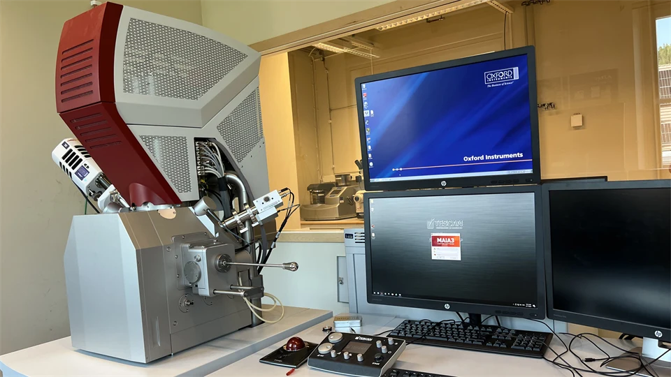
A scanning electron microscope (SEM) uses an electron beam to create detailed, high-resolution images of material surfaces. The beam scans across the sample, and the reflected signals reveal the surface’s structure and composition.
In materials science, SEM is essential for analyzing the microstructure of metals, fractures in materials, or surfaces of composites.
The technique is also used to investigate defects in materials, such as cracks in steel or irregularities in ceramics, which is important for improving durability and performance in constructions or electronic products.